Summary: The clock driver circuit of a CCD scanner is the 'heartbeat generator' that turns the image information captured by the silicon chip into a readable electrical signal. It is responsible for generating multi-phase clock signals with precise timing, sufficient amplitude, and necessary overlap, driving the charge packets accumulated under each pixel electrode to 'leapfrog' step by step toward the output amplifier. Without this analog circuit, no matter how excellent the photosensitive performance of the CCD is, it cannot output a single usable pixel. This article will start from the working principle of the clock driver, and through specific examples from industries such as barcode scanning, document digitization, industrial inspection, astronomical observation, and medical imaging, elaborate on how this seemingly obscure analog circuit determines the success or failure of the entire scanning system. At the end of the article, a detailed summary will be provided, outlining the key technical points and their interrelationships. |

|
23. The CCD Clock Driver: The Analog Heartbeat Behind Every Scan |
1. Why a CCD Needs a Clock Driver: Starting from the 'Bucket Brigade' |
The photosensitive area of a CCD is essentially an array of tiny capacitors. When photons fall on the silicon surface, they excite electrons, which accumulate in the 'potential well' beneath each pixel electrode. The depth of this potential well is controlled by the voltage applied to the electrode above it. The stronger the voltage, the deeper the well, and the more charge it can hold. |
But accumulating charge is only half the job. An image sensor must eventually read out the charge of each pixel in some order, otherwise it is just a piece of silicon that has been 'stained' by light. The genius of CCD lies in its ability to transfer charge packets from one electrode to the next, much like a bucket brigade passing water buckets hand to hand. To achieve this, at least two, and typically three or four, clock signals with different phases are needed. These signals take turns going high and low, causing the potential wells to move in a coordinated manner: the well under the previous electrode becomes shallower, while the well under the next electrode becomes deeper, and the charge packet 'slips' into the new position. |
The job of the clock driver circuit is to generate these multi-phase signals. It must ensure that the signals have sufficient amplitude to create a sufficiently deep potential well, typically requiring voltages between 5 volts and 12 volts. It must also ensure that adjacent phases have a certain degree of overlap in timing, so that when the previous well is disappearing and the next well has already been established, the charge has a place to go. If there is a gap between two phases, the charge packets will be trapped in no man's land and cannot be transferred completely, causing 'lag' or 'transfer loss'. |
This may sound simple, but in reality it is one of the most demanding analog design challenges in the entire scanner system. The clock driver must drive a capacitive load with considerable parasitic capacitance, while maintaining fast edge rates, minimal ringing, and extremely low noise. In a barcode scanner, it must also respond to different readout rates under various ambient light conditions. Next, we will enter specific industry scenarios to see how this circuit works in practice. |
|
2. Retail and Logistics: The Invisible Workhorse Behind Barcode Scanners |
2.1 Supermarket Checkout Counters: The Clock Driver Inside a Linear CCD |
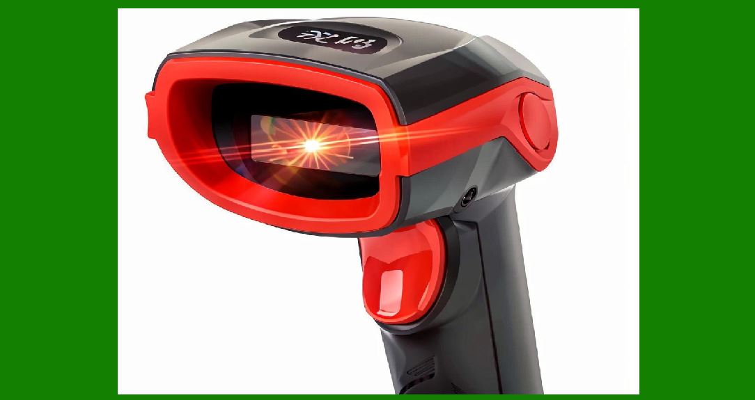
The scanner at a supermarket checkout counter is where most people first encounter CCD technology. This device typically uses a linear CCD array, meaning the photosensitive area is a row of pixels, not a two-dimensional array. When scanning a barcode, a red laser or LED line is projected onto the barcode, and the reflected light is imaged onto the linear CCD through a lens. The barcode's black and white bars are converted into strong and weak electrical signals on the CCD, and then the clock driver pushes these signals out in sequence. |
Toshiba's TCD1103GFG is a typical linear CCD sensor for barcode scanning applications. It requires external clock signals to operate, and the clock driver circuit must be designed according to the sensor's timing requirements. In a handheld scanner, the clock driver must operate stably under battery-powered conditions, because the supply voltage may drop as the battery discharges. If the clock amplitude is insufficient, the potential well becomes too shallow to accommodate the charge generated by strong reflected light, and the signal will saturate and distort. If the clock edge is too slow, charge transfer will be incomplete, leaving residual charge from the previous pixel and causing blurred barcode edges. |
More critically, barcode scanners need to handle barcodes in motion. When the cashier swipes an item across the scanning window, the relative speed between the barcode and the scanner may vary. Some scanners use a phase-locked loop to dynamically adjust the CCD's clock frequency based on the detected barcode movement or ambient light conditions. The PLL controller switches the frequency dividing ratio according to the control data, thereby changing the clock signal frequency output to the CCD. This means that the clock driver is not outputting a fixed frequency, but must be able to respond to instructions at any time to accelerate or decelerate the charge transfer rhythm. For the clock driver, this is like driving a car while frequently shifting gears, and each shift must be smooth without stalling. |
|
2.2 Warehouse Sorting Lines: The Challenge of High-Speed Readout |
In large logistics distribution centers, barcode scanners on sorting lines face completely different challenges from supermarket checkout counters. Packages pass by on conveyor belts at speeds of one to two meters per second, and each package may have multiple barcodes facing different directions. These industrial scanners typically use CCD arrays with higher pixel counts and require clock drivers to support faster readout rates. |
When the line speed increases, the time the CCD can integrate per line becomes shorter, and the charge packets become weaker, placing higher demands on the clock driver's noise performance. Any clock feedthrough or power supply ripple coupled to the CCD output will drown out the weak signal. Therefore, the clock driver in industrial scanners usually adopts measures such as separate power supply filtering, shielding, and ground isolation to prevent clock noise from contaminating the analog signal path. |
Another practical issue is heat. Industrial scanners often need to operate continuously for long periods, sometimes in environments with poor ventilation. The clock driver itself is a power amplifier circuit, and its efficiency directly affects the temperature rise of the entire unit. Early designs using linear amplifiers had significant heat generation, while later designs gradually introduced more efficient drive architectures, reducing quiescent current while maintaining sufficient drive capability. |

|
3. Document Digitization: The Clock Driver's Role in Scanners and Copiers |
3.1 Flatbed Scanners: How Slow Scanning Achieves High Quality |
The working method of a flatbed scanner is fundamentally different from that of a barcode scanner. It scans a stationary document line by line with very high pixel counts, often reaching thousands or even tens of thousands of pixels per line. The linear CCD used in document scanners, such as Toshiba's TCD1710DG, emphasizes high sensitivity, high resolution, and wide dynamic range. The clock driver must drive a longer CCD shift register, and the total capacitance of the clock line is correspondingly greater. |
In flatbed scanners, scanning speed is not the primary consideration; image quality is. The clock driver can afford to use a lower clock frequency to reduce noise and power consumption. But low frequency brings another problem: the charge transfer time becomes longer, and the effect of dark current becomes more significant. Dark current is the charge generated by thermal excitation even without light illumination, and it accumulates over time, creating a gray fog-like background in the image. The clock driver's timing design must leave sufficient margin for charge transfer, while not making the integration time too long. |
The clock driver in document scanners also faces mechanical challenges. The scanner's optical carriage moves along a guide rail, and the cable connecting the CCD to the main board must withstand millions of bends. The clock signal lines are part of this cable, and any intermittent contact or increased impedance will cause the clock waveform to deteriorate, manifesting as periodic streaks or missing lines in the scanned image. A good clock driver design takes this into account by providing sufficient drive current margin at the output stage to overcome the additional losses introduced by long cables. |
3.2 High-Speed Document Scanners: Balancing Speed and Fidelity |
In check processing systems in banks or high-volume document archiving scenarios, scanners need to process hundreds of pages per minute. At this point, the CCD readout rate must be increased to several times that of ordinary flatbed scanners. The rise and fall times of the clock driver become critical: if the edges are too slow, the charge transfer time window will be compressed; if the edges are too fast, it will excite ringing on the clock line, and the overshoot of the ringing may cause charge injection or alter the potential distribution on the silicon surface. |
Experienced analog designers will carefully tune the output stage of the clock driver at this point, using methods such as series resistance damping or snubber networks to suppress ringing while maintaining acceptable edge rates. Sometimes two clock drivers with different drive capabilities are used: one for the faster horizontal shift register and another for the relatively slower vertical transfer. This 'differentiated drive' approach, while increasing circuit complexity, allows each clock path to operate at its optimal operating point. |

|
4. Industrial Inspection: The Clock Driver's Requirements Under Extreme Conditions |
4.1 Production Line Defect Detection: No Compromise on Stability |
In factories producing LCD panels, metal foils, or plastic films, machine vision systems inspect surface defects on continuously moving materials. The linear CCD cameras used in these systems are essentially the same as those in scanners, but the operating environment is completely different. Vibration, temperature fluctuations, dust, and electromagnetic interference are all commonplace. |
The clock driver circuit must operate stably over a wide temperature range. The mobility of silicon decreases at low temperatures, and the switching speed of the driver's internal transistors decreases accordingly; at high temperatures, leakage currents increase. The clock waveform optimized at room temperature may exhibit insufficient edge rates at low temperatures or increased noise at high temperatures. Industrial-grade clock drivers require thorough temperature compensation design or the selection of components with wider tolerances. |
Another requirement for industrial inspection is long-term consistency. A scanner used for defect detection may need to operate continuously for years, and the judgment threshold of the vision algorithm is calibrated based on the camera's stable output. If the clock driver's amplitude or timing drifts over time, the calibration will become invalid, leading to false positives or missed detections. Therefore, the reference voltage source inside the clock driver must have extremely low long-term drift, and key parameters of the drive stage cannot degrade significantly with age. |
4.2 Semiconductor Wafer Inspection: When the Clock Driver Meets Nanometer Precision |
Semiconductor wafer inspection is one of the most demanding application scenarios for CCD clock drivers. Wafer inspection systems need to detect defects of tens of nanometers in size, and the pixel count is extremely high, sometimes requiring the stitching of multiple CCD chips to complete the scan. The clock driver must drive very long shift registers with total clock line capacitance that can be several times that of ordinary scanners. |
In this scenario, the clock driver's noise performance is pushed to the limit. The charge signal generated by a single photon or a small number of electrons must be faithfully transferred without being contaminated by any clock coupling. Patent literature mentions that in semiconductor inspection and metrology systems, custom waveform generators are placed as close as possible to the image sensor to minimize distortion and crosstalk of clock signals during transmission. This 'distributed clock driver' architecture requires the integration of multiple waveform generators into a single integrated circuit, placing them right next to the CCD chip. This approach is much more complex and costly than conventional approaches, but for wafer inspection applications, it is the only way to achieve the required signal-to-noise ratio. |

|
5. Astronomy and Space Observation: The Clock Driver Under Extreme Reliability Requirements |
5.1 Ground-Based Telescopes: Driving CCDs at the Summit of Mauna Kea |
Large astronomical telescopes use CCD cameras to capture light from distant galaxies. These CCDs are often cooled to minus 100 degrees Celsius or even lower to reduce dark current to negligible levels. At such low temperatures, the characteristics of semiconductor devices change significantly. The clock driver must be able to operate normally in this extreme environment, or be placed in a warm area outside the dewar, with signals transmitted to the CCD inside the dewar through vacuum feedthroughs. |
The challenge of long-distance transmission is that the clock line's capacitance increases, and the driver needs greater output current. At the same time, the transmission line's reflections and attenuation distort the waveform. Astronomers have extremely high requirements for image quality; any clock-induced charge injection will manifest as spurious signals in the image, and these spurious signals may be mistaken for actual celestial objects. Therefore, the clock driver design for astronomical CCDs places special emphasis on waveform purity and repeatability, and sometimes multiple rounds of testing and calibration are required to ensure that the clock edge shape is consistent under different operating conditions. |
5.2 Space Missions: How the Clock Driver Works in Orbit |
The CCDs used in space telescopes, such as the Hubble Space Telescope, must withstand the radiation environment of space. High-energy particles bombarding the silicon chip create charge traps that capture electrons during charge transfer, causing charge transfer inefficiency (CTI). The clock driver cannot directly repair radiation damage, but by adjusting the clock timing and amplitude, the impact of traps can be partially mitigated. For example, appropriate overlap and slower edges can give trapped charge more time to be released, reducing residual signals. |
The Chandra X-ray Observatory experienced accelerated degradation of its CCD performance in orbit due to radiation damage, manifested as significant charge transfer inefficiency. Engineers on the ground improved the imaging quality by lowering the focal plane temperature and developing complex CTI correction models. If the clock driver's timing is designed with sufficient flexibility, it can provide an additional adjustment dimension for in-orbit calibration. This reminds us that the design of the clock driver is not only a hardware issue but also needs to leave room for coordination with the software correction algorithms. |

|
6. Medical and Scientific Imaging: Where Clock Driver Precision Equals Diagnostic Accuracy |
6.1 Microscopy and Pathology Slides: Faithfully Reproducing Every Detail |
In digital pathology, glass slides are scanned at high magnification into gigapixel images for pathologists to review on monitors. The linear or area CCDs used in these scanners require clock drivers that provide extremely uniform charge transfer. If the clock amplitude or edge timing varies across different regions of the CCD, the brightness of the image will be uneven, and subtle cellular structures may become indistinguishable. |
The clock driver in pathology scanners also needs to coordinate with the mechanical scanning stage. The scanning stage moves in precise steps, and the CCD simultaneously performs line-by-line readout. If there is jitter or phase error in the clock signal, the stitched image will show 'stitching' artifacts, and pathologists may mistake these artifacts for tissue abnormalities. Therefore, the clock driver's timing is typically locked to the scanning stage's encoder signal to ensure synchronization between image acquisition and mechanical motion. |
6.2 Spectral Instruments: Clock Noise Becomes Spectral Noise |
In spectrophotometers and Raman spectrometers, CCDs are used to detect the intensity distribution of light at different wavelengths. The charge packets on each pixel correspond to a narrow spectral band. The clock driver's noise, if coupled into the charge transfer process, will manifest as random fluctuations in the spectral baseline, reducing the instrument's detection limit. |
Toshiba's TCD1103GFG is also listed as suitable for spectrophotometer applications. In spectral instruments, the clock driver's requirements for low noise are even stricter than those for barcode scanners. Any periodic clock feedthrough will appear as spurious peaks at specific frequencies in the spectrum, interfering with the identification of trace components. Designers typically use linear power supplies to power the clock driver, avoiding the switching noise of DC-DC converters, and also physically isolate the clock driver from the CCD analog output stage. |

|
7. Detailed Summary |
Returning to the core argument of this chapter: the CCD clock driver is not a dispensable peripheral circuit but the key link that determines whether charge packets can be transferred losslessly from the silicon chip to the outside world. It must simultaneously satisfy three seemingly contradictory requirements: sufficient amplitude to create a sufficiently deep potential well, precise overlap and edge timing to ensure complete charge transfer, and sufficiently low noise so as not to contaminate the weak signal itself. |
From the application examples in this article, we can see that different industries have vastly different priorities for the clock driver. Retail barcode scanners pursue cost, power consumption, and adaptability to dynamic scanning; document scanners pursue image uniformity and long-term stability; industrial inspection pursues reliability under extreme temperatures and vibrations; semiconductor inspection pursues ultimate signal-to-noise ratio; astronomy pursues waveform purity and radiation environment adaptability; medical imaging pursues consistency with mechanical scanning and spectral fidelity. These demands drive the clock driver to evolve in different directions: some applications require highly integrated single-chip solutions, while others require discrete designs with carefully selected components. |
A common thread running through all these scenarios is that the clock driver is an analog circuit, and its performance cannot be fully simulated and verified by digital means. The shape of the clock waveform, the degree of ringing, the coupling of power supply noise, and the parameter drift of devices with temperature and age all require designers to understand the physics of the silicon chip and the actual operating environment of the system. This is precisely the underlying reason why 'from photons to bits' is not a simple digital transformation process: before the bits are generated, the analog clock driver is already writing the fate of the signal with voltage and time. |
For engineers designing CCD scanning systems, the lessons of this chapter are: treat the clock driver as a core component of the system, not as an afterthought circuit that can be casually handled with a general-purpose driver chip. Its power supply, grounding, layout, and heat dissipation all require the same level of attention as the CCD itself. When the scanned image exhibits unexplained streaks, lag, or noise, the first place to check is often not the optical path or the sensor, but the clock signal that is driving the entire bucket brigade. |
 cs@easiersoft.com